Kepler Computing targets AI memory bottleneck with new chip architecture
The startup says its 3D-stacking and ferroelectric technologies could increase HBM and SRAM density using existing fabs, but commercial scale remains unproven.
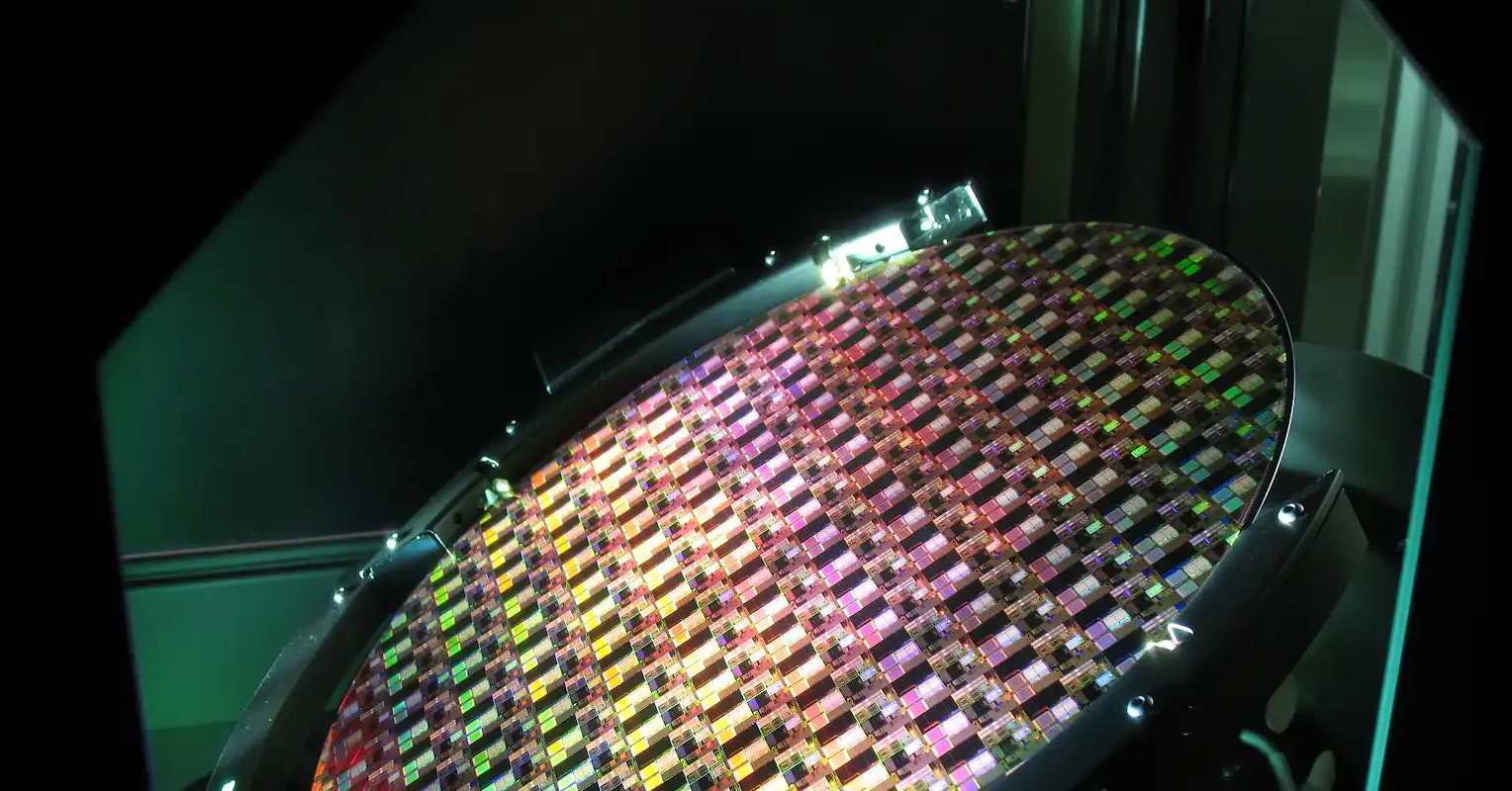
Kepler Computing has emerged from stealth with a memory-chip design it says could ease supply constraints driven by artificial-intelligence demand. The startup claims its 3D-stacking and proprietary ferroelectric-material technologies can increase the density of high-bandwidth memory (HBM) and SRAM without extreme ultraviolet lithography.
The approach is designed to work with existing semiconductor facilities. HBM uses stacked DRAM and is increasingly important in AI data centres, while SRAM is typically integrated into processors including CPUs, GPUs and XPUs. Kepler says its architecture can fit more memory within a fixed footprint and reduce the energy required to move data between memory and compute.
According to WIRED, Kepler has raised US$468 million from investors including GlobalFoundries, Intel Capital, AMD Ventures, Baillie Gifford and Bill Gates’ Gates Frontier fund. The US Department of Commerce has committed up to US$245 million to support the company’s US development of high-performance AI memory technology.
Kepler is conducting testing with GlobalFoundries in Singapore and Vermont and says it converted a development fab in eight months. The company has run its technology on about 2,000 wafers and plans to ship initial HBM samples later in 2026, increase Singapore production in 2027 and begin US chip production in 2028.
The claims come as SK Hynix, Micron and other major memory manufacturers invest billions of dollars in new fabs to meet demand for HBM. Kepler’s proposition is that adapting existing facilities could expand supply without waiting for entirely new plants.
The technology still faces significant manufacturing risks. Kepler has not disclosed the composition of its proprietary material and has yet to demonstrate full-scale production, yields or commercial performance across millions of devices. GlobalFoundries says contamination controls and dedicated equipment will be essential, while a chip analyst cited by WIRED was not briefed on Kepler’s technology.