Samsung and TSMC commit to ASML’s High NA EUV chip technology
Samsung plans to use the technology for DRAM production by 2028, while TSMC targets advanced-node manufacturing from 2030.
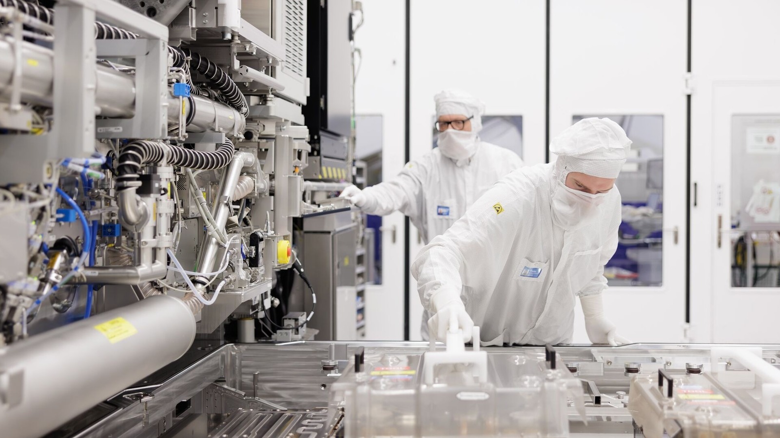
Samsung and Taiwan Semiconductor Manufacturing Co. will adopt ASML’s High NA extreme ultraviolet lithography technology, joining Intel as reported users of the advanced chipmaking equipment.
Samsung plans to use the technology in DRAM production by 2028. TSMC intends to deploy it in advanced-node manufacturing from 2030, although both dates remain company targets and could be affected by technical or production bottlenecks.
ASML is also working with Samsung and TSMC on 12-inch photomasks, which are intended to improve fab productivity, increase yields, lower costs and remove stitching constraints. Existing photomasks are typically six inches.
The larger masks are designed to help manufacturers print finer features on larger chips without stitching sections together, a process that adds complexity and cost. SK Hynix is evaluating whether to join the initiative.
ASML expects to begin testing 12-inch photomask fabs in 2031, with production forecast to start in 2033. Intel is currently the only reported company deploying High NA EUV, using it on its 18A process for selected Panther Lake processors.