IBM unveils nanostack chip technology to extend Moore’s Law
The company claims the sub-nanometre architecture could add a decade to semiconductor roadmaps, though physical transistor spacing remains unchanged.
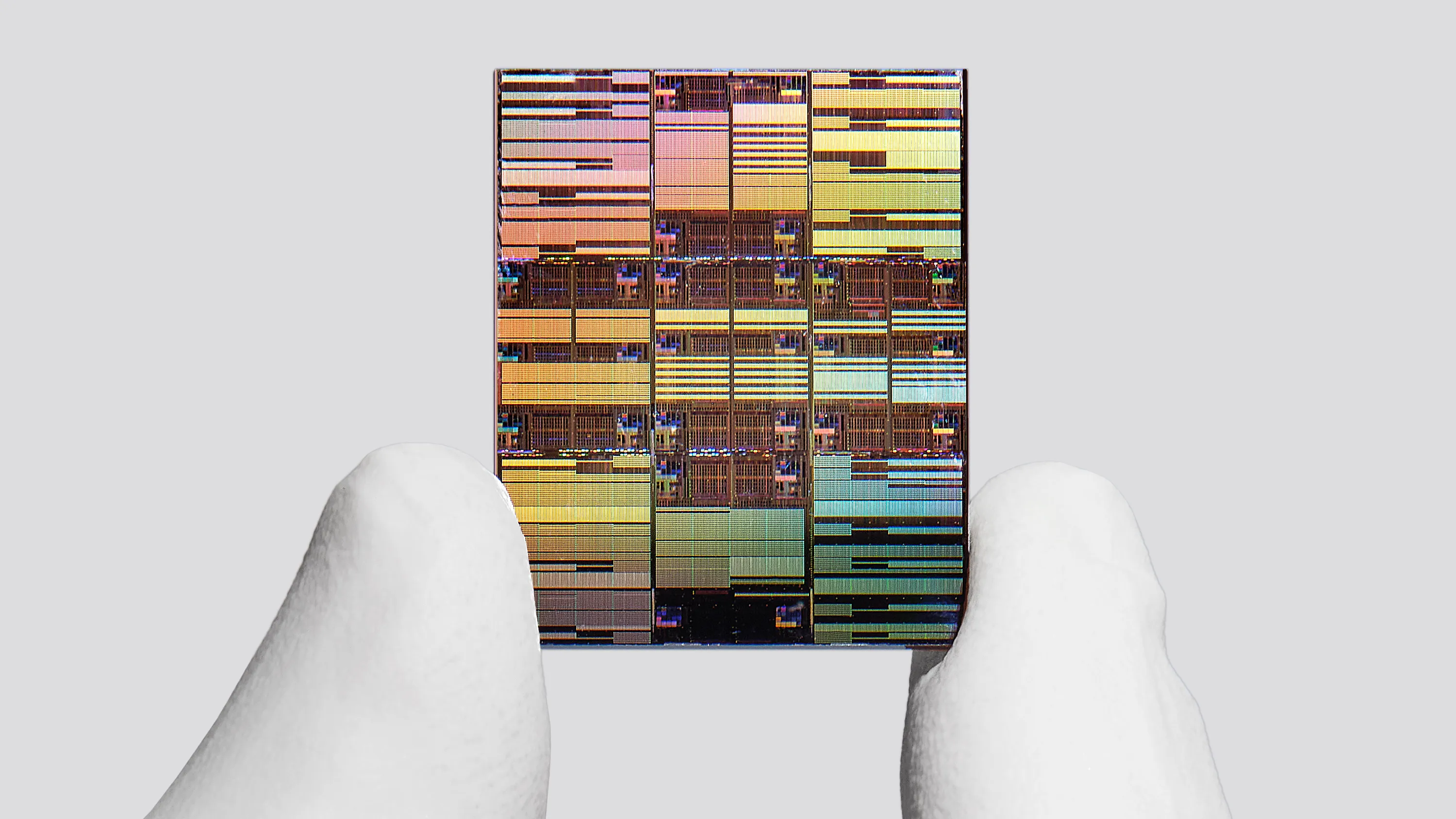
IBM has unveiled a prototype chip utilising a 'nanostack' architecture that vertically stacks transistors, a move the company claims could extend Moore’s Law by another decade. The new design features approximately 100 billion transistors on an area the size of a fingernail, achieving twice the density of IBM’s previous state-of-the-art technology announced in 2021. The approach, known as complementary field-effect transistor (CFET) nanostacking, allows chips to perform up to 50% more work in the same time and be up to 70% more energy efficient.
The architecture addresses a physical limit reached by traditional chipmaking, where transistors have shrunk to sizes where quantum mechanics interferes with their function. Rather than continuing to shrink components horizontally, engineers are pivoting to vertical stacking. IBM’s method involves fabricating transistors on one silicon layer, placing a second silicon layer on top, and then fabricating another layer of transistors directly on top of that before creating electrical connections between the layers.
IBM’s design distinguishes itself from competitors like Intel, Samsung, TSMC, and Imec by staggering the second layer of transistors rather than sitting them directly on top of the first. This staggered configuration simplifies wiring and improves alignment, which is critical given the microscopic scale of the components. The channel in IBM’s nanostack approach consists of three nanosheets, each 15 atoms thick, spaced nine nanometers apart.
The company refers to its technology as a “sub-nanometer” or “0.7 nanometer” node, following industry conventions for naming generations. However, this is a marketing term and does not correspond to physical characteristics; the actual distance between transistors remains around 40 nanometers. IBM has reportedly solved the “thermal budget” challenge by ensuring the manufacturing process for the second stack remains below 400°C, though the specific methods remain undisclosed.
IBM plans to partner with semiconductor manufacturers to produce the chips, with expectations for widespread use in data centres within a decade. The technology is expected to be deployed in various chip types, including GPUs and CPUs, to help facilities better manage energy consumption as computing demands increase.