ASML ships $400 million lithography machines to sustain AI chip dominance
Intel has acquired the first unit for testing in Oregon, but high costs and geopolitical restrictions are reshaping the global semiconductor landscape.
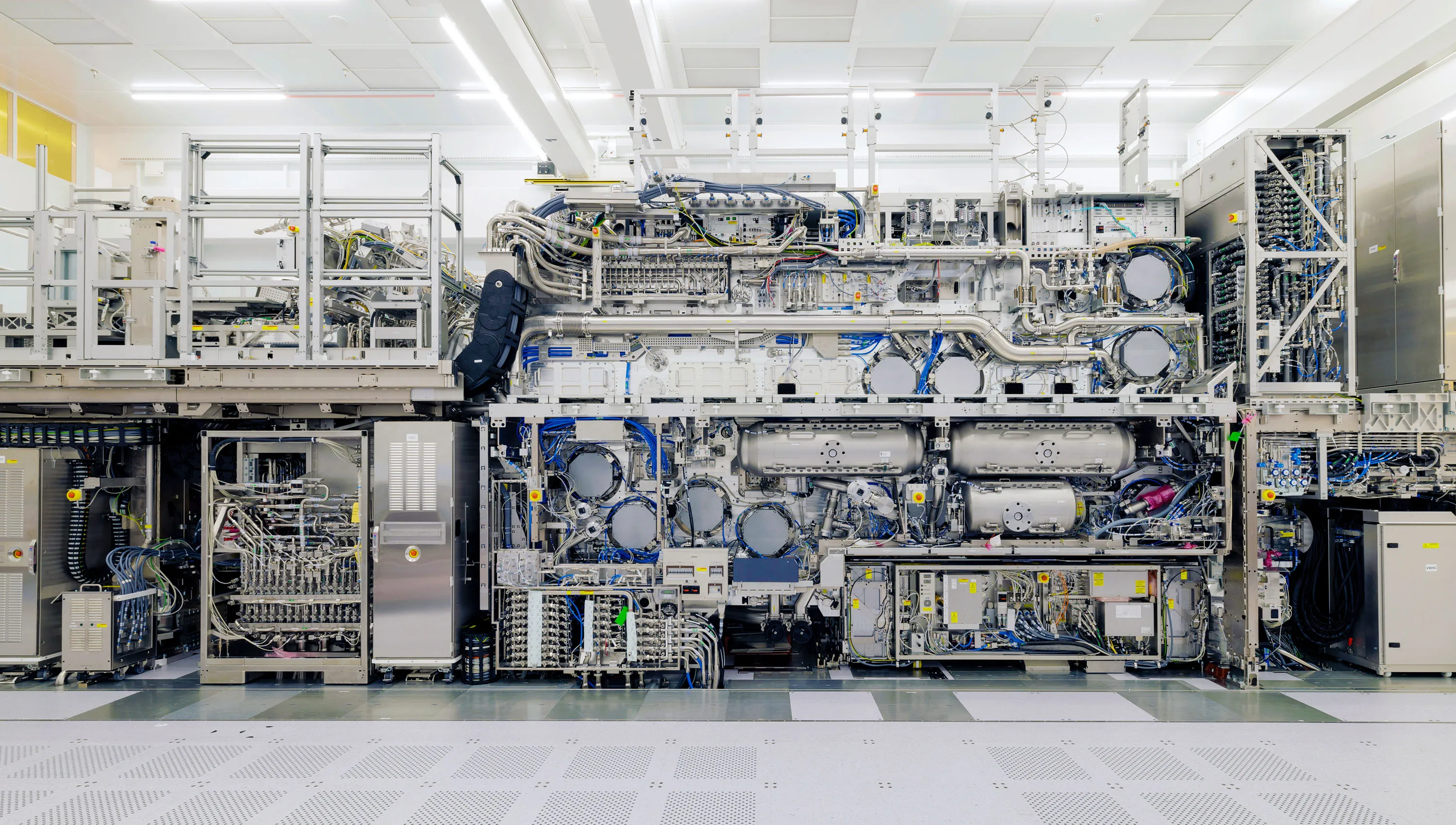
Dutch semiconductor equipment manufacturer ASML has commenced shipping its latest high-numerical-aperture (high-NA) extreme-ultraviolet lithography machines, priced at $400 million each. The technology achieves an eight-nanometer resolution, a significant advancement from the previous 13-nanometer standard, enabling the production of denser chips essential for artificial intelligence applications. The company sold nearly 50 EUV machines in 2025, generating nearly $40 billion in revenue, with a market capitalisation exceeding half a trillion dollars.
Intel purchased the first high-NA machine for testing at its Oregon facility in spring 2024, with observers expecting chip production to begin in the following year. The company plans to ease the technology into use, initially utilising it for precision components before expanding its role in manufacturing. This move is part of Intel’s broader strategy to recapture market share in the foundry business, aiming to compete directly with TSMC and Samsung by offering customers the ability to print tiny patterns faster and with greater simplicity.
Competitors such as TSMC are delaying adoption of the high-NA technology due to its high cost, preferring to extend the capabilities of existing EUV tools. TSMC stated it will deploy the machines when they are mature and ready to deliver maximum benefit, with some analysts suggesting serious volume deployment may not occur until the 2030s. The industry has historically shifted paradigms only when existing methods can no longer be extended, and TSMC is likely to push multi-patterning techniques further before committing to the new, expensive hardware.
Geopolitical tensions have restricted ASML’s sales of high-end machines to China, prompting Beijing to invest heavily in domestic alternatives. Since 2019, the US government has pressured the Dutch government to impose an embargo on ASML’s high-end tools to prevent China from developing advanced AI chips. In response, China is pouring billions into replicating ASML’s technology, while also leveraging deep-ultraviolet lithography and developing lighter-weight large language models to compensate for hardware limitations.
Startups including Substrate and Lace Lithography are developing competing lithography technologies to challenge ASML’s market dominance. Substrate aims to produce chips at $10,000 per wafer by 2030 using x-ray lithography from a particle accelerator, while Lace Lithography plans to use helium atom beams by 2029–2030. Despite these emerging threats, ASML engineers continue to refine their technology, with a “hyper-NA” design potentially offering six-nanometer resolution expected for volume sales in the second half of the 2030s.